
NEWS
ASML Ties Its India Growth to Tata’s First Fab
ASML has opened a 20-to-30-person India office and says any scale-up waits on Tata Electronics’ 2028 Dholera fab hitting yield on time.

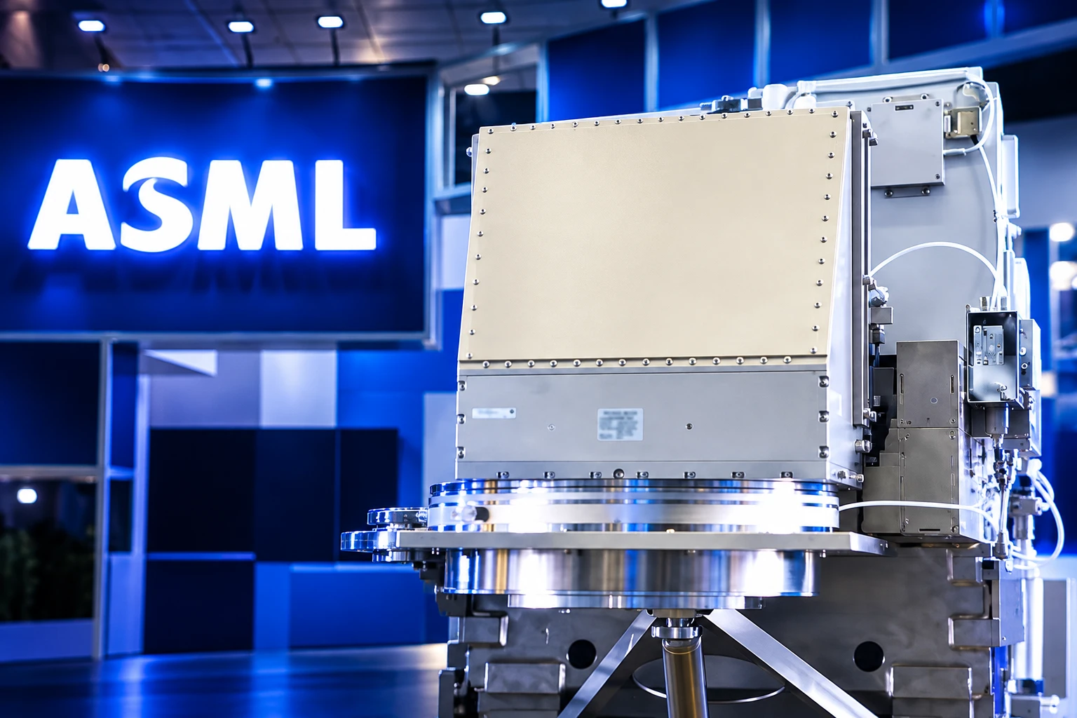
ASML has started India operations with a plan to hire 20 to 30 engineering graduates, tying any larger presence to Tata Electronics. The Dutch lithography supplier said at SEMICON India 2026 that the office exists because Tata is its first 300 mm customer in India.
How fast that team grows, said Lin Kiat Yap, ASML’s head of customer support, “really depends on the ambitions of India, and it really depends on the ambitions of Tata.”
How Many People Is ASML Hiring in India?
ASML will begin with 20 to 30 young engineering graduates. Yap, speaking on the sidelines of the New Delhi show, said the company is starting “right now” and will “see how fast it scales.” That is a customer-support beachhead, not a plant.
The company’s own release for the event, held from 17 to 19 September 2026 at booth 602, said that since a May 2026 memorandum with Tata Electronics it has established a legal entity in India and is setting up a customer support office. The same note puts global headcount at more than 44,000 full-time staff, based in Veldhoven in the Netherlands.
ASML’s public directory still lists more than 60 locations worldwide and does not yet name an Indian city. The office is being stood up because a customer finally appeared, not because the firm is moving production.
ASML’S FOOTPRINT AGAINST THE INDIA OFFICE
- India start: 20 to 30 engineering graduates for customer support.
- Global staff: More than 44,000 full-time employees, per ASML’s 17 September 2026 release.
- Factories: Over 7,000 people in seven cleanroom plants in the EU, the US and Asia.
- Veldhoven: Almost 3,000 staff in two factories assembling EUV and DUV lithography systems.
Wayne Allan, ASML’s chief strategic sourcing and procurement officer, put the logic in one line at the show: the company did not have a semiconductor customer in India, and now it has Tata. Field engineers follow tools. They do not precede them.
Tata’s Dholera Fab Carries the Scale-Up
Tata Electronics is building India’s first commercial 300 mm silicon fab at Dholera in Gujarat, with Taiwan’s Powerchip Semiconductor Manufacturing Corporation as technology partner. Planned capacity is 50,000 wafers a month. The project is publicly costed at Rs 91,000 crore (about $11 billion).
Allan told the conference Tata is the first customer in India with a 300 mm plant of that size. The process menu on the record runs 28 nm, 40 nm, 55 nm, 90 nm and 110 nm, mature and specialty nodes aimed at cars, power chips, phones, communications and industrial parts, not the leading-edge AI logic that needs extreme ultraviolet tools.
Yap was blunt about why that single line matters to ASML. He wants Tata to succeed so a second player, then a third, will look at India more closely. The 20-to-30-person office is a wager that Dholera becomes that proof, not a claim that India already has a lithography industry.
We want to make Tata successful because I think when people see Tata being a success, I think people will start to spend a little bit more time, be a little bit more focused in India and see the potential opportunities.
Lin Kiat Yap, executive vice president and head of customer support, ASML, on the sidelines of SEMICON India 2026
Randhir Thakur, Tata Electronics’ chief executive, said at the same event that the Dholera fab and the company’s packaging plant in Assam are on track against commitments made to the government. Allan said Tata is on schedule on those commitments. Commercial output is still guided to 2028.
DHOLERA, ON THE NUMBERS ASML IS UNDERWRITING
| Item | Figure |
|---|---|
| Wafer size | 300 mm |
| Monthly capacity | 50,000 wafers |
| Project cost | Rs 91,000 crore (about $11 billion) |
| Process nodes | 28 nm to 110 nm |
| Technology partner | PSMC, Taiwan |
| Guided commercial start | 2028 |
| ASML India starting staff | 20 to 30 engineers |
Allan also put a market size on the bet. He said India’s semiconductor market could reach around $120 billion by 2030, against global demand of at least $1.6 trillion. That is demand. It is not installed wafer capacity, which still hangs on this first 300 mm line.
Lithography Tools Are Due in Late 2027
ASML is putting staff, warehousing and service kit into Gujarat ahead of the tools themselves. Allan said the company will ship lithography systems to the Dholera site in the second half of 2027, and that it is getting support on the warehousing it needs in the area.
That date sits between the May 2026 memorandum and the 2028 production guide. The machines have to be installed, qualified and yielding before Tata can show the “good quality and yield” Allan said other customers will watch. He said time to market is what those customers look for, and that a clean run at Dholera would draw more of them to India.
THE DATES ON ASML’S INDIA BET
- May 2026: ASML and Tata Electronics sign a memorandum covering lithography for the 300 mm Dholera fab, plus talent, suppliers and research work.
- 17 September 2026: ASML says it has formed an Indian legal entity and is setting up a customer support office, and exhibits at SEMICON India in New Delhi.
- Second half of 2027: Allan says lithography tools ship to Gujarat.
- 2028: Tata’s plant is guided to begin commercial operations, the test ASML has tied to any larger India scale-up.
Christophe Fouquet, ASML’s chief executive, said in September 2025 that the company had no immediate plans for manufacturing or research in India while it set up a customer support office. A year later the office is opening and the factory answer has not changed.
Why ASML Will Not Build a Factory Yet
Allan was asked about making lithography systems in India. He left a question mark on it. The company enters a region to support customers and to hire local engineers, he said, and a supply base has to exist before anyone talks about a plant.
Then at some point, we may very well be looking at manufacturing. I see there’s a question mark there because there’s no plans for that as it stands at present.
Wayne Allan, chief strategic sourcing and procurement officer, ASML, at SEMICON India 2026
That stance matches how the company is built. Assembly of EUV and DUV scanners is concentrated in Veldhoven, with other modules and optics in places such as Wilton, San Diego, Berlin and Taiwan. ASML says over 7,000 people work in seven cleanroom factories in the EU, US and Asia. India is being added as a support node on the Tata account.
Allan said ASML is still new to India’s industrial base and is talking to peers such as Applied Materials and Lam Research about what can be bought locally. Cleaning, coating and the tight tolerances chip plants need are the gaps he named. Aerospace, auto and general machining exist. Turning that into parts that sit inside a scanner is a different job, and he put it after the first fab, not before.
A 20-to-30-person hire plan is the size of a field-service crew for one customer, which is exactly what Dholera is until another 300 mm plant is announced. The sarcastic reading of that headcount is also the accurate one: this is not a factory announcement wearing a press-conference suit.
India Wants a Dozen Fabs by 2035
Allan repeated the government’s own arithmetic. India’s projection, he said, is to make 15 per cent to 25 per cent of its local semiconductor demand in domestic wafer fabs by 2032, which “means you’re going to have to have several fabs by 2032.” The longer target he cited was 35 to 50 per cent of demand made locally by 2035, which he said implies about a dozen plants with large capacity.
India currently has one commercial 300 mm silicon fab under construction. The first phase of the India Semiconductor Mission approved 12 manufacturing units with combined investment of more than Rs 1.64 lakh crore, on a scheme outlay of Rs 76,000 crore. Most of those units are packaging, compound or specialty lines, not a row of 300 mm silicon foundries.
The Union Cabinet cleared Semicon 2.0 in July 2026 with an outlay of Rs 1.27 lakh crore (about $13.5 billion). The notified programme covers chip design, equipment and materials, more fabs, packaging, research and skills. Union minister Ashwini Vaishnaw said at SEMICON India the government had already seen investment interest of $11-12 billion under the new scheme, spanning equipment, materials, gases, chemicals and substrates, with companies to name themselves as boards approve.
Allan’s “several fabs by 2032” line only works if Dholera is not a one-off. He said if India is going to scale, “we need to be able to build many fabs here,” and that policy from Prime Minister Narendra Modi’s government plus engineering talent is why ASML is willing to staff Gujarat at all.
Other states are already trying to peel off the non-fab work. Karnataka’s industries minister, M.B. Patil, said his team met an ASML delegation during the show, including Joost Stienen, Herman Boom, Frank Heemskerk, Yogesh Sadarangani and Joost van Hees, and asked the company to look at the state for engineering, software, training and related work. That pitch can run even if every scanner still ships from Veldhoven.
The 363-Acre Park Beside the Fab
Tata is trying to put the missing suppliers next to the plant rather than wait for them to appear. Utpal Shah, senior vice president for strategy and business development at Tata Electronics, said the Dholera fab will have about 450 suppliers, a mix of Indian and foreign firms, and that they need some presence close to the line because a fab “cannot be down even for a few hours.”
The company is developing a 363-acre plug-and-play vendor park in Dholera with Singapore’s Ascendas First Space, with power, water, roads and, in some cases, building shells. Thakur said Tata would sign 16 agreements at the conference with firms from Europe, Japan, Singapore and India. Around 56 memorandums were signed across the event as a whole.
WHAT HAS TO SIT NEXT TO DHOLERA
- Supplier count: About 450 vendors supporting the fab, per Shah.
- Vendor park: 363 acres with Ascendas First Space, sold as plug-and-play plots beside the plant.
- Materials: Fujifilm has signed to put a semiconductor-materials plant in Dholera with phased investment of about Rs 800 crore.
- Uptime rule: Shah said the capital-heavy line cannot be down for even a few hours, which is why vendors have to live next door.
Allan said the first 300 mm fab has to test, qualify, hold yield and hit its schedule so there are no delays. If that run is clean, he expects more of ASML’s customers to spend time on India, which is the only path from 20 to 30 people to a staff that looks like a real country office. If it slips, the legal entity and the warehouse in Gujarat still exist, and the factory question mark stays on the whiteboard.
The next hard date is not a speech in New Delhi. It is a crate of lithography tools due in Gujarat in the second half of 2027, and a Dholera line that has to yield in 2028 on the calendar Tata already gave the government.

Edinburgh Opens a 2027 Tour Built for Time Trials

Korda Maps Auður From Meðalland to Irvine Bay

Apple Music Films Its New Logo in Mineral Oil

Oppo Prices the Pad Mini Above India’s iPad Mini

Austen Soaks Scotland Before Boelo Brings Weekend Gales

Volkswagen Sells the Osnabruck Plant to Clear a Board Fight

Apple’s Foldable iPhone Hinges on Samsung Display Supply

Saksham Gaur Finds He Is His Own Company’s Client

Tata Motors’ Iveco Tender Opens as Holders Still Decide

Onimusha Way of the Sword Preload Hits a Windows 11 Wall
-
 AUTO2 months ago
Volkswagen Sells the Osnabruck Plant to Clear a Board Fight
-
 NEWS2 months ago
Apple’s Foldable iPhone Hinges on Samsung Display Supply
-
 AUTO2 months ago
Tata Motors’ Iveco Tender Opens as Holders Still Decide
-
 BUSINESS2 months ago
Saksham Gaur Finds He Is His Own Company’s Client
-
 GAMING2 months ago
Onimusha Way of the Sword Preload Hits a Windows 11 Wall
-

 ENTERTAINMENT3 years ago
What is SD on Amazon Prime? – All You Need to Know
-

 BUSINESS2 months ago
Hyderabad 22-Carat Gold Jumps After a False Bargain
-

 NEWS2 months ago
iQOO 16 Locks 8,400 mAh While 100W Charging Holds