
 Ishan Crawford
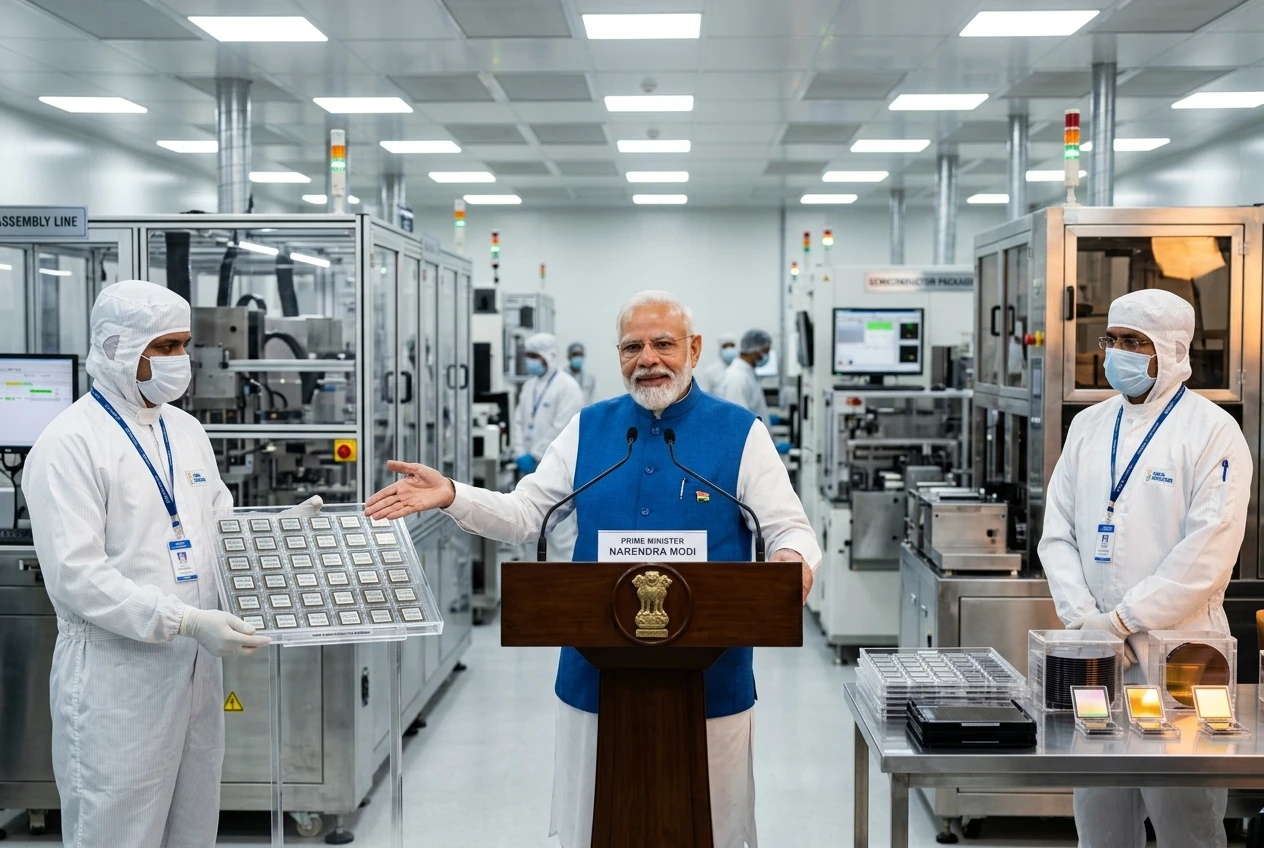
 On Saturday, India’s Sanand semiconductor cluster gained a third commercial chip plant when Prime Minister Narendra Modi inaugurated CG Semi’s Rs 7,600 crore packaging facility. The plant, built by a joint venture of India’s CG Power and Industrial Solutions, Japan’s Renesas Electronics and Thailand’s Stars Microelectronics, can produce up to 300 million packaged chips a year at full capacity. Its first batch was bound for Japan.
“Every industrial superpower has developed through clusters. America has Silicon Valley. Sanand is moving in the same direction. One industry attracts another, creating jobs and pulling in suppliers,” Modi told the gathering at the July 4 ceremony. Modi’s framing borrowed from older industrial history, where chip clusters in the United States, Taiwan and Japan took decades to mature.
Modi’s Third Commercial Chip Plant
CG Semi’s G1 facility was inaugurated in August 2025 and spent the months that followed on equipment installation, process stabilisation, workforce training and customer qualification before commercial production began on July 4. A second unit, G2, is under construction on the same site and will expand capacity once commissioned.
Modi’s description of the cluster’s growth borrowed from the older playbook of state-led industrial policy. “Step by step, brick by brick, chip by chip,” he said, quoting the Semicon India programme’s slogan. Union Electronics and Information Technology Minister Ashwini Vaishnaw said chips from the G1 plant would be exported to Japan, the United States and Europe, and that India is now expected to have five operational semiconductor facilities by the end of 2026, against an earlier target of four.
Today is a proud moment for Micron and India’s growing semiconductor industry. This pioneering facility, the first assembly and test site of its kind in the country, helps build a resilient ecosystem that underpins the global AI economy.
Sanjay Mehrotra, Chairman, President and CEO of Micron Technology, made the remarks at the company’s Sanand opening on February 28, 2026.
Combined with Micron’s $2.75 billion assembly and test facility, which opened on February 28, 2026 with more than 500,000 square feet of cleanroom space, and Kaynes Semicon’s OSAT line, which began pilot production in April 2025 and shipped India’s first commercial multi-chip module to California’s Alpha & Omega Semiconductor (AOS) in October 2025, Sanand now has three chip plants operating on three distinct business models. A fourth project, Tata Electronics’ fabrication plant at Dholera, is rising 50 kilometres north with first silicon targeted for the end of 2026.
The Back End of Chipmaking
The work at Sanand sits in the back end of chipmaking. Assembly, test, marking and packaging, known in the trade as ATMP or OSAT, takes finished silicon wafers, dices them into individual chips, bonds them to carriers, encases them in protective shells and runs electrical checks before they ship. It is not the front end, where raw wafers are etched with circuitry in fabrication plants (fabs) that require billions of dollars and years to build.
Packaging is the cheaper place to start. Building a fab takes years and far more capital than an OSAT line; a packaging facility costs a fraction of that cost and ramps in months. Malaysia and Vietnam have done packaging competently for decades without ever becoming Taiwan, and that record is the obvious objection to reading Sanand as the start of a cluster. The less obvious counter is that packaging forces an entire workforce and supplier base to learn the unforgiving disciplines of the industry, from cleanroom protocol to yield management and tolerances measured in billionths of a metre, before any fab is bolted down.
| Plant | Partner tech providers | Back-end function |
|---|---|---|
| CG Semi (G1) | Renesas (Japan), Stars Microelectronics (Thailand) | OSAT packaging, test and marking |
| Micron Sanand | Micron’s global DRAM and NAND wafer network | Memory ATMP into finished modules |
| Kaynes Semicon | Alpha & Omega Semiconductor (US), Mitsui (Japan) | Multi-chip module packaging |
How Older Clusters Started
Silicon Valley took shape around a university. Frederick Terman, Stanford’s engineering dean, spent the 1940s and 1950s pushing students to start companies nearby and leasing them land in a new industrial park. Cold War defence spending quadrupled Stanford’s federal research income in a single decade, and a missiles-and-space contractor became the largest employer in Santa Clara County. When William Shockley brought the transistor west in 1956 and eight of his engineers defected to found Fairchild Semiconductor, the recirculation began: Fairchild begat Intel, Intel begat a hundred others, and a venture capital industry grew up on Sand Hill Road to fund the next wave.
Taiwan’s Hsinchu Science Park was more deliberate. Inaugurated in 1980 and modelled on Stanford’s research park, it sat next to two elite universities and, crucially, a government research institute, ITRI, that worked as an incubator. ITRI licensed chip technology from the United States, then spun its own people out into private companies. The most consequential was TSMC, spun off in 1987 under Morris Chang, a Texas Instruments veteran the Taiwanese government had recruited to run ITRI. Chang’s bet, that a company could make only the chips other firms designed, the pure-play foundry model, was met with scepticism and went on to give Taiwan a single firm producing more than 90% of the world’s most advanced chips.
Japan offers two more variations. Kyushu, in the country’s south west, earned the nickname Silicon Island when Mitsubishi and NEC built wafer fabs there in the 1960s, and by the 1980s the region hosted more than a hundred chip-related firms before the industry drifted to cheaper Korea and Taiwan. It is reviving now because the existing water, suppliers and trained hands let TSMC reach mass production in Kumamoto within two years of breaking ground. Tsukuba, the planned science city north of Tokyo, contributes something different: not volume manufacturing but upstream research, with about thirty institutes and twenty thousand researchers generating the materials science and metrology the industry runs on.
Put all of this together and the pattern is consistent. Clusters need an anchor, a fab or a research institute, around which suppliers and talent thicken. They reward pre-existing industrial infrastructure. They depend on the free movement of skilled people. The timeline runs in decades.
Dholera Fills in the Map
Fifty kilometres north of Sanand, Tata Electronics is building India’s first commercial fabrication plant at Dholera, with Taiwan’s Powerchip Semiconductor Manufacturing Corporation (PSMC) providing the technology and execution support. Total investment is up to Rs 91,000 crore, with manufacturing capacity of up to 50,000 wafers per month, and the project is expected to generate more than 20,000 direct and indirect skilled jobs.
The fab will run on mature nodes, with the Tata release naming 28nm, 40nm, 55nm, 90nm and 110nm processes. Chips manufactured there are aimed at power management ICs, display drivers, microcontrollers and high-performance computing logic, with markets in automotive, computing, data storage, wireless communication and artificial intelligence. The partnership with PSMC gives Tata access to a broad portfolio across leading edge and mature nodes, though the Dholera plant itself is built for high volume manufacturing on the larger geometries.
Tata Electronics has targeted first silicon at Dholera for the end of 2026. If those wafers are then finished on Sanand’s packaging lines, the two would operate as a single supply chain.
Three Hundred Thousand Engineers, Waiting
India is home to nearly 20% of the world’s chip design engineers, according to the India Semiconductor Mission, working in design houses of Qualcomm, Nvidia, AMD, Intel, Broadcom and MediaTek clustered around Bengaluru, Hyderabad and Noida. Indian engineering teams have contributed to chip designs at the two-nanometre frontier, the most advanced node in commercial development anywhere. India has the engineering talent to design chips. What has held the country back is the ground on which to build them, and a domestic supply chain to commercialise them under Indian brands. NITI Aayog’s roadmap betting on packaging argues the country should focus on the back end of chipmaking rather than try to match Taiwan and South Korea at the leading edge.
A numbered timeline of Sanand’s chip milestones makes the speed visible.
- April 2025: Kaynes Semicon pilot production begins at its Sanand OSAT facility.
- August 2025: CG Semi’s G1 plant is inaugurated, ahead of equipment installation and customer qualification.
- October 2025: Kaynes ships India’s first commercial multi-chip module, 900 intelligent power modules with 17 dies each, to California’s AOS under a five-year supply agreement for 10 million chips a year.
- February 28, 2026: Micron opens its Sanand assembly and test facility, with first made-in-India memory modules shipped to Dell Technologies.
- July 4, 2026: CG Semi begins commercial production, the third commercial chip facility in Sanand.
The Risks That Don’t Disappear with Speed
India has design talent in abundance. It still lacks equivalent depth in fab operations and advanced process engineering, and industry estimates on India’s specialist gap warn of a shortfall of 250,000 to 300,000 skilled professionals by 2027. India imports the overwhelming majority of its chipmaking equipment, its speciality chemicals and its ultra-pure gases; over 90% of essential semiconductor inputs are sourced from abroad.
The binding constraint is execution. In the near term, Dholera needs to achieve first silicon on schedule and the Sanand plants need to ramp from pilot lines to their promised volumes with real global customers. The medium-term question is whether a genuine supplier base, the chemicals, the gases, the equipment servicing, thickens around these anchor plants. Over the longer term, the question is whether India climbs from mature-node packaging toward advanced manufacturing and reduces the dependence on imported tools and materials.
India Semiconductor Mission 2.0 budget details describe a scheme designed to strengthen chip design, equipment manufacturing, logistics and material supply. For now, the geography has changed. Three commercial plants are running in Sanand, a fab is rising 50 kilometres north at Dholera, and the design talent remains in place. The remaining question is whether the supply chain compounds the way older clusters did.
Frequently Asked Questions
When did CG Semi begin commercial production?
CG Semi began commercial production at its G1 packaging plant in Sanand on July 4, 2026, Prime Minister Narendra Modi’s office confirmed at the inauguration. The G1 plant is the first of two units in a planned Rs 7,600 crore investment, with G2 under construction.
How many chip plants are running in Sanand?
Three. CG Semi’s G1 packaging plant began commercial production on July 4, 2026. Micron’s assembly and test facility opened on February 28, 2026. Kaynes Semicon’s OSAT line began pilot production in April 2025 and shipped its first commercial multi-chip module in October 2025.
What will the Dholera fab make?
The Dholera fab, built by Tata Electronics in partnership with Taiwan’s Powerchip Semiconductor Manufacturing Corporation, will run on mature nodes of 28nm, 40nm, 55nm, 90nm and 110nm. Chips are aimed at power management ICs, display drivers, microcontrollers and high-performance computing logic.
Will India make leading-edge chips?
Not on the present roadmap. India’s first commercial fab targets mature nodes rather than the most advanced manufacturing processes. A leading-edge fab is far more capital-intensive and depends on equipment that is itself tightly held technology.
When will Dholera produce its first chips?
First silicon is targeted for the end of 2026, according to Tata Electronics’ public statements. The plant has been under construction since 2024 in partnership with Taiwan’s Powerchip Semiconductor Manufacturing Corporation.
How much has India committed to semiconductors?
India Semiconductor Mission 2.0 was proposed to strengthen chip design, equipment manufacturing, logistics and material supply, according to statements from the Prime Minister’s office. Four major semiconductor projects have been approved: CG Semi, Micron, Kaynes Semicon and Tata’s Dholera fab.
 moto g77 POWER Launches in India at Rs 23,999 With 7,000mAh Battery
  Beats Power Pink Woven Cables: Specs, Price, and Color Match Play
  Redmi Note 17 Series Confirmed for July 14 China Launch
  Meta’s Glasses Update Guards the Camera, Not the Bystander
  India’s Retail GCC Hub Now Outscales Five Peers Combined
  Dundee to Host First Scotland StreetCar Festival Alongside Eco Rally