
 Ishan Crawford
 India’s Union Cabinet cleared seven infrastructure and manufacturing decisions worth ₹2,19,353 crore, roughly $26 billion, on Wednesday, anchored by a ₹1.27 lakh crore semiconductor bet. Prime Minister Narendra Modi chaired the meeting. Ashwini Vaishnaw, the Union minister for railways and for electronics and IT, announced the package right after.
The chip mission carries the biggest number and the longest history. Its first round lost the Vedanta-Foxconn joint venture to a very public withdrawal and struggled with fab infrastructure gaps. The sequel arrives four times the size of the ₹76,000 crore the government set aside the first time.
Seven Decisions Land in a Single Cabinet Meeting
Vaishnaw laid out the list at a press briefing after the Cabinet and the Cabinet Committee on Economic Affairs (CCEA) met under Modi’s chairmanship.
I am presenting before you the seven major decisions taken by the Cabinet and the Cabinet Committee on Economic Affairs under the chairmanship of Prime Minister Narendra Modi.
Vaishnaw said this at the post-Cabinet briefing in New Delhi.
| Decision | Scale | What It Covers |
|---|---|---|
| Semicon 2.0 Mission | ₹1,27,500 crore | Chip design, fabs, packaging and R&D across the value chain |
| Mobile Phone Manufacturing Scheme | ₹62,500 crore | Second round of production-linked incentives for handset makers |
| Varanasi NH-19 to Ring Road corridor | ₹14,447.64 crore | 46.039-km six-lane elevated link with a cable-stayed bridge |
| Varanasi Varuna riverbank corridor | ₹10,998.32 crore | 6-/4-lane elevated road along the Varuna river |
| National Investment Policy for Urea-2026 | 9 new plants | Targets 1 crore tonnes of additional domestic urea capacity |
| Paradeep-Haridaspur rail doubling | ₹2,542 crore | Second track on the Odisha freight line |
| Dangoaposi-Rajkharsawan fourth line | ₹1,365 crore | Fourth track through the Jharkhand-Odisha mineral belt |
Six of the seven carry their own price tag. Add them up and the total lands almost exactly on the ₹2,19,353 crore Vaishnaw announced, since the urea policy works through plant-level investment commitments rather than a single Cabinet-approved outlay.
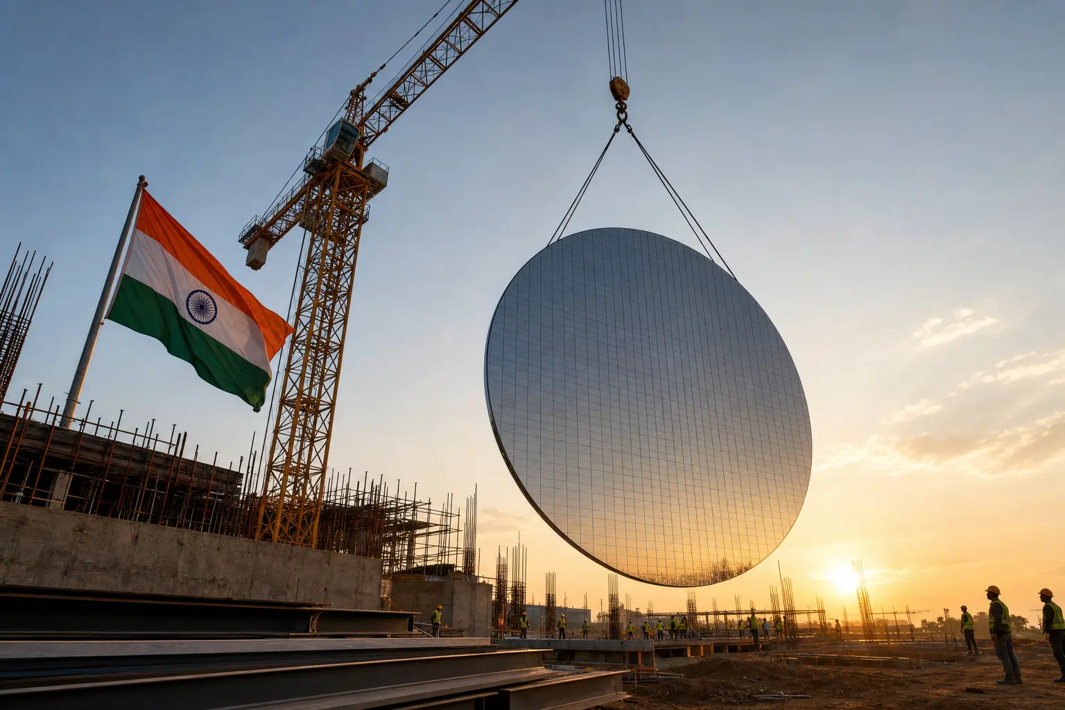
The Chip Mission Gets a Rewrite
Semicon 2.0, formally the second edition of the India Semiconductor Mission, got the largest single number of the day: ₹1,27,500 crore, more than four times its predecessor’s budget.
Where Semicon 1.0 Stumbled
The original mission carried a ₹76,000 crore incentive framework run by the Ministry of Electronics and Information Technology. It has since backed 12 projects worth a combined ₹1.64 lakh crore, government figures show, and helped train the design workforce the new phase leans on.
The debut also exposed weak points. A Carnegie Endowment review of the mission’s progress points to the Vedanta-Foxconn joint venture’s collapse as its most visible setback, alongside quieter problems: costly land and power, patchy fab-grade infrastructure, and continued reliance on imported manufacturing tools India still cannot make itself.
The mission happens to land the same week global chip stocks wobbled elsewhere. In Seoul, a chip-sector selloff tripped the KOSPI’s circuit breaker even after Samsung posted a record quarterly profit, a reminder that scale alone does not shield the industry from demand swings.
Six Pillars Behind the New Money
The new mission spans the entire chip supply chain rather than just fabrication, according to the government’s official account of the approval. It rests on six pillars:
- Strengthening the chip design ecosystem, including intellectual property and design tools
- Incentivising manufacturers of the equipment, materials, chemicals and gases that feed a fab
- Adding new fabrication plants, with the next new fab targeted for 2028
- Building up ATMP/OSAT capacity, the back end of chip manufacturing that packages finished wafers
- Funding semiconductor research and development
- Training the workforce a chip industry needs, from technicians to design engineers
- ₹4 lakh crore in fresh investment the government expects Semicon 2.0 to draw in over its lifetime
- ₹2 lakh crore worth of semiconductor production it is targeting from that investment
- 68,000 students already trained in chip design across 315 universities under the mission’s first round
- 105 startups and MSMEs given access to industry-standard chip design software so far
None of those figures, on their own, build a fab. The other six decisions Vaishnaw announced spend closer to the ground.
A ₹62,500 Crore Sequel for Mobile Manufacturing
The Mobile Phone Manufacturing Scheme takes ₹62,500 crore into a second round of production-linked incentives for handset makers, extending a programme credited with turning India into a major phone assembly base.
Pankaj Mohindroo, chairman of the India Cellular and Electronics Association, has said the government’s continued backing signals manufacturing-led growth in electronics and semiconductors through scale and policy continuity. Ashok Chadak, president of the India Electronics and Semiconductor Association, has pointed to the scheme’s expanded coverage, including equipment, materials, chemicals, design tools, R&D and workforce training, as evidence the plan gives industry room to commit capital with confidence.
Some of that expansion already has a number attached. The Electronics Component Manufacturing Scheme, a component-level incentive sitting alongside Semicon 2.0, saw its outlay doubled to ₹40,000 crore in this year’s budget, an infrastructure wager Finance Minister Nirmala Sitharaman placed months before Wednesday’s Cabinet meeting.
Two Elevated Corridors Rise Along Varanasi’s Rivers
Varanasi, the prime minister’s own Lok Sabha constituency, gets two of the seven approvals. The bigger one is a 46.039-km link corridor connecting National Highway-19 with the Varanasi Ring Road: a six-lane elevated carriageway with a cable-stayed bridge and an extradosed foot-over-bridge-cum-major bridge, plus loops, ramps, link roads and service roads along the Ganga riverbank.
It will be built under the Hybrid Annuity Model (HAM), which pays developers partly during construction and the remainder afterward, at a total cost of ₹14,447.64 crore. That includes ₹6,037.85 crore for civil construction, excluding GST and including utility shifting, and ₹541.11 crore for land acquisition.
The second Varanasi project runs along the Varuna riverbank: a 6-/4-lane elevated corridor with its own ramps and loops, also under HAM, priced at ₹10,998.32 crore. Together the two corridors are meant to pull through-traffic off Varanasi’s older streets as the pilgrim city keeps growing.
Where Does the Rest of the Money Go?
The last two decisions cover fertiliser and rail freight. The National Investment Policy for Urea-2026 clears nine new plants aimed at one crore tonnes of additional domestic urea capacity, while doubling the Paradeep-Haridaspur line and adding a fourth track between Dangoaposi and Rajkharsawan expand freight capacity across Odisha and Jharkhand for a combined ₹3,907 crore.
The urea policy is the only one of the seven built around a production target rather than a rupee figure: nine plants, one crore tonnes, aimed at cutting India’s dependence on imported fertiliser. The two railway projects are smaller but concrete. Track doubling between Paradeep and Haridaspur costs ₹2,542 crore; the fourth line between Dangoaposi and Rajkharsawan, a stretch serving the mineral belt straddling Odisha and Jharkhand, costs ₹1,365 crore.
What Could Still Sink the Bet
Money was never the mission’s first problem. Semicon 1.0 had ₹76,000 crore and still lost its flagship fab project. Researchers at the IMPRI Impact and Policy Research Institute point to the same structural gaps going into round two: expensive land and power, a shortage of fab-grade infrastructure, and a skilled workforce that exists on paper more than on factory floors.
India trains roughly a fifth of the world’s chip design engineers, that research notes, yet still struggles to convert design talent into people who can run a fabrication line. Tool and process know-how remains largely imported, a dependency Semicon 2.0’s pillars target directly but cannot fix by decree.
- Industry groups, including the India Cellular and Electronics Association and the India Electronics and Semiconductor Association, call the expanded outlay proof of continuity that gives manufacturers confidence to keep investing.
- Researchers at Carnegie and IMPRI point to unresolved fab infrastructure gaps and import dependence on foreign tools as the mission’s harder, unfinished half.
- Both sides agree the design talent exists on paper; they disagree on how fast that talent converts into finished fabs.
The roadmap is specific about where it wants to land. The mission’s published targets call for advanced manufacturing at the 3-nanometre and 2-nanometre nodes, domestic capability to cover seventy to seventy-five percent of India’s own chip demand by 2029, and a place among the world’s top semiconductor nations by 2035. The government has set aside ₹1,000 crore for the mission’s first year, FY2026-27, with the next new fab targeted to come online in 2028.
Frequently Asked Questions
When did India launch its first Semiconductor Mission?
The Union Cabinet approved the original India Semiconductor Mission in December 2021 with a ₹76,000 crore incentive framework, administered by the Ministry of Electronics and Information Technology, the same ministry running Semicon 2.0.
How many chip design projects has the mission already backed?
Twenty-four semiconductor design projects have received financial support under the mission so far, part of the groundwork the government points to heading into Semicon 2.0.
How is Semicon 2.0 different from the Mobile Phone Manufacturing Scheme?
The two sit at different points of the same supply chain. Semicon 2.0 funds chip design, fabrication and packaging, while the Mobile Phone Manufacturing Scheme’s ₹62,500 crore supports the assembly and export of finished handsets.
How much of the package goes to Uttar Pradesh?
Just over ₹25,000 crore, the two Varanasi corridors combined, is earmarked for Uttar Pradesh alone, more than the two railway projects and the urea policy combined.
What do ATMP and OSAT mean in chip manufacturing?
ATMP stands for assembly, testing, marking and packaging, and OSAT for outsourced semiconductor assembly and test; both describe the back-end work that turns a finished silicon wafer into a packaged chip ready for a phone or a car, a stage India already handles better than front-end fabrication.
 Scotland’s Facial Recognition Push Sparks Mask Ban Call
  Galaxy Z Flip 8 Hits $799 Only If Your Trade-In Qualifies
  If England Had Kept Water Public Like Scotland
  Samsung Smart Switch Now Moves Passwords and eSIM From iPhone
  Old Firm Spend Pulls Clear as Premiership Rivals Patch Squads
  Chinese Studios Quietly Seize the Gamescom Stage